VERSATILE SIGNAL PROCESSOR CARD
INTRODUCTION
The field of signal processing has growing enormously since past decade. Signal processing has wide applications in a number of fields like RADAR and SONAR technology, communications, speech and video processing, seismology and a many more. Although many signal-processing systems can be most economically implemented with analog methods, it is the capability of digital systems to achieve guaranteed accuracy and reproducibility. This specific reason encouraged developers and scientists to make advancements in this field. The cost of the hardware involved is high enough that hinder hobbyists and amateur developers to work in this field. Unavailability of the appropriate hardware is also a common problem in our country. A low cost and easy to construct Signal Processing circuit is a solution to these problems.
Versatile Signal Processing Card uses the processing power of your computer that is almost sufficient for maintaining desired level of accuracy. The driving software is designed in assembly language that makes the circuit ideal for real time processing. A number of different programs can be created in almost every low-level language or high-level languages to drive the circuit and accomplish desired job. The card can work on any operating system. The versatile nature of this card can be noticed by some of the below mentioned uses of the circuit. This circuit may be used as:
*Developers can also find out many more interesting and efficient uses of this card.
INTERFACING
The card is interfaced to the computer using ISA bus slots provided in almost all personal computers based on i386 or higher processors. Although ISA slots are discontinued in the latest motherboards (based on Intel 815 chipset or above). ISA bus is very common to most of the electronic and computer hobbyists. It is simple to understand and easy to use.
THE ISA BUS
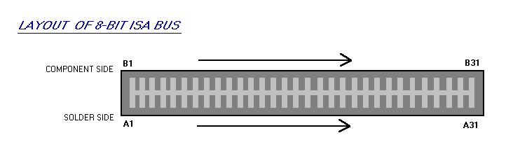
The ISA (Industry Standard Architecture) bus has evolved from original 8 bit standard to the 16 bit standard as we found it today. The ISA expansion slot resembles the tongue and groove system with total 62 contacts, 31 each side. The slot provides eight data lines, 20 address lines and some control lines. The figure below shows the pin orientation of ISA bus slot.
Any ISA card can operate at a maximum frequency of 8.33 MHz. It provides a maximum bandwidth (data transfer rate) of 8M/sec. Nowadays motherboards come with 16 bit wide ISA bus slots that could support both 8 bit and 16 bit cards. One can plug an 8-bit card into the forward part of the slot. The slot has standard dimensions so the card must also have standard dimensions for plugging it into the slot. The dimensions of 8-bit ISA cards are as follows:
4.2 inches (106.68mm) high
13.13 inches (333.5mm) long
0.5 inch (12.7mm) wide
ADDRESS DECODING
This card is interfaced to computer on isolated IO scheme for data transfer between CPU and I/O devices. The card uses 15 address lines for address decoding. The address is decoded by 74LS154 (4 to 16 line demultiplexer) and 7420 (Dual 4 input NAND gate). The decoding scheme is as follows:
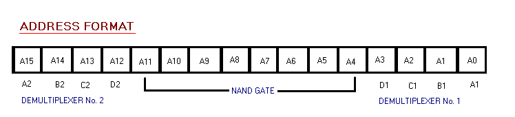
For the outputs of the two NAND gates to be low, it is essential that address lines A11-A4 must be high. Hence, the address for the three devices viz. ADC, DAC and Control Register is of the value XFFXh (h denotes that the value is in hexadecimal number). To solve resource conflicts due to port address jumper J1- J4 can be used. It allows you to select one of the four addresses as listed below:
|
DAC |
ADC |
Control Register |
|
|
J1 SHORTED |
0FF0h |
0FF1h |
0FF2h |
|
J2 SHORTED |
4FF0h |
4FF1h |
4FF2h |
|
J3 SHORTED |
2FF0h |
2FF1h |
2FF2h |
|
J4 SHORTED |
6FF0h |
6FF1h |
6FF2h |
Three inverters are used to invert the output of the demultiplexer, as the chip enable pins of DAC, ADC and control register are active high.
SAMPLING
Sampling is an essential criterion for any digital signal processing system. The quality of the processing system greatly depends upon the sampling rate.
SAMPLING RATE
To obtain or reconstruct analog signals out of its digital signals properly it is essential that the sampling rate must be greater than twice of the maximum frequency component. (As stated by Nyquist theorem)
To understand this phenomenon let us look at an example:
If a sampling system is designed to obtain 1000 samples of the analog input signal in one second then the maximum frequency that can be used is 500Hz.
WORKING (HARDWARE)
TRANSCEIVER
IC 74LS245 is used as a transceiver that acts a bridge between CPU and ADC and DAC.
It sends or receive data according to the value of signal S/~R. Hence this pin is connected to the ~IOW and ~IOR signals via AND gate as shown in the schematic diagram.
CONTROL REGISTER
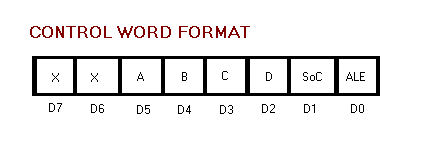
An octal latch IC 74LS373 is used as a control register to control the working of the ADC. An appropriate control word must be placed in this register in order to ensure proper working of the ADC. The control word is used to select proper channel for analog input signal. Control register makes this card very useful as one can easily program the card in various ways. Control register also controls the ‘Start of Conversion’ signal and Sample and Hold circuit necessary for initiating the conversion. Format of the control register is as shown in the figure.
DIGITAL TO ANALOG CONVERTER
The task of digital to analog conversion is done by IC 0800. It is a monolithic type DAC. The input to IC 0800 is given by octal latch IC 74LS373. It is operated in its standard mode. This device provides output corresponding to the value of binary input.
ANALOG TO DIGITAL CONVERTER
IC 8016 is 16 channel analog to digital converter. It converts analog signal into equivalent 8-bit digital output. It uses successive approximation technique for conversion. A sample and hold circuit is connected across its MULTIPLEXER OUT pin and COMPARATOR IN pin. The device works at a clock frequency of 640KHz and consumes about 100s for conversion. The clock pulse for the device is derived from the ISA slot’s pin number b20 that provides clock pulses at 8.33MHz. To achieve the clock of 640 kHz a mod 13 counter is used. ADC is selected by the computer by providing an active high signal at OUTPUT ENABLE pin. To select the channels of ADC, the EXPANSION CONTROL pin is tied with +5 V power supply. The ALE and Start of Conversion (SoC) is provided by the control register (IC 74LS373). Whereas the End of Conversion (EoC) signal is applied to interrupt request (IRQ 3).
Note: IRQ 4, IRQ 5, IRQ 6, or IRQ 7 may also be used if resource conflict occurs.
SAMPLE AND HOLD CIRCUIT
A sample and hold circuit is employed in this project to maintain proper sampling at high frequencies also. IC LM 398 works as a sample and hold circuit. When a logic high signal is placed on the LOGIC HIGH pin, it goes to sampling condition. As the pin goes low the circuit moves to hold position. The sampling period of the IC is the time gap between the arrival of SoC signal after EoC signal. The hold time is equal to the conversion period, hence an appropriate ‘value of hold’ capacitor is used.
CLOCK GENERATION
ADC 8016 requires clock pulses for its operation. For this purpose, we derive clock pulses from the motherboard. Pin number b20 of ISA slot is the CLOCK pin (this pin provides clock at 8.33 MHz in a 16-bit ISA slot whereas it provides the clock at 4.77 MHz in an 8-bit ISA slot). ADC 8016 works at an optimal frequency of 640 kHz. To achieve this a frequency divider circuit is used. This small circuit block is comprised of a binary counter (IC 7493), an AND gate (IC 7421) and an inverter (IC 7404). The circuit is a mod-13 counter.
CALCULATIONS:
b. 4.77 MHz / 7 = 681 kHz (Approx.) [for 8-bit ISA slot]
To achieve proper clock frequency a mod-7 counter or a mod-13 counter must be used. This variation in the circuit may be possible due to variation in computer hardware in an individual computer. Although most of the PCs nowadays have 16-bit ISA slots.
WORKING (SOFTWARE)
Different software can be developed various languages in both high-level and low-level languages (although assembly language is preferable because of faster execution and small size). Software (and updates) for different applications of this card will be provided time to time.
The card can turn your computer into a digital oscilloscope. For this, a program ‘oscill.exe’ is developed in assembly language. The program is designed with modular approach to improve performance. Different procedures are used for performing various tasks. For simplicity in program, ‘input channel 0’ is only used.
To plot the waves or electric signals, the display is to graphical mode. Different graphical modes can be used with 16 color (in both VGA and SVGA mode) or 256 color (only available in SVGA mode). This program uses BIOS interrupts and provides direct access to display. To initialize graphical mode, function call 00h and video mode 12h for 640 by 400 resolution (16 colors), is used. For initializing display in SVGA mode, function call 4F02h and video mode 102h (16 colors) or 103h (256 colors) with a resolution of 600 by 800, can be used.
NOTE: Some of the display adapters may not work properly in SVGA mode.
The changes made in video settings and interrupt vector are restored before the control is given to operating system.
This program produces sinusoidal waveform of any desired frequency. The frequency can be set by providing suitable count, used for providing delay between reflection of two sample values to the D/A converter section of the card. The values of the digital samples are stored in a data buffer called ‘Sintab’. These values are repeatedly supplied to the D/A converter at regular intervals of time.
The calculation for time delay is as follows:
Total time of the delay =
S Machine Cycles ´ Number of InstructionsOutput Frequency = Time Delay
´ Number of SamplesThis program uses only D/A converter section of the circuit. To stop the generation of sinusoidal waveform one must follow the on screen instruction.
PARTS LIST
IC
7402
7404
7420
7421
7432
7493
74LS154
74LS 245
74LS373
DAC 0080
ADC 8016
LM 398
2.5K
0.1
mFIC Bases PCB Jumpers Connecting Wires